Table of Contents
A chip application is mostly figures. The claims recite a gate dielectric, a barrier liner, a doped well, and every one of those features has to appear somewhere a draftsperson can point to. That makes semiconductor patent drawings a different problem from the mechanical figures most drawing guides are written around: the subject matter is layered, the critical dimensions are nanometres, and the honest answer to “what does it look like?” is often a grey electron micrograph rather than a line drawing. The rules were not written with a 3 nm FinFET in mind, but they still govern. Here is how the seven that matter most actually apply.
Why semiconductor patent drawings break the usual rules
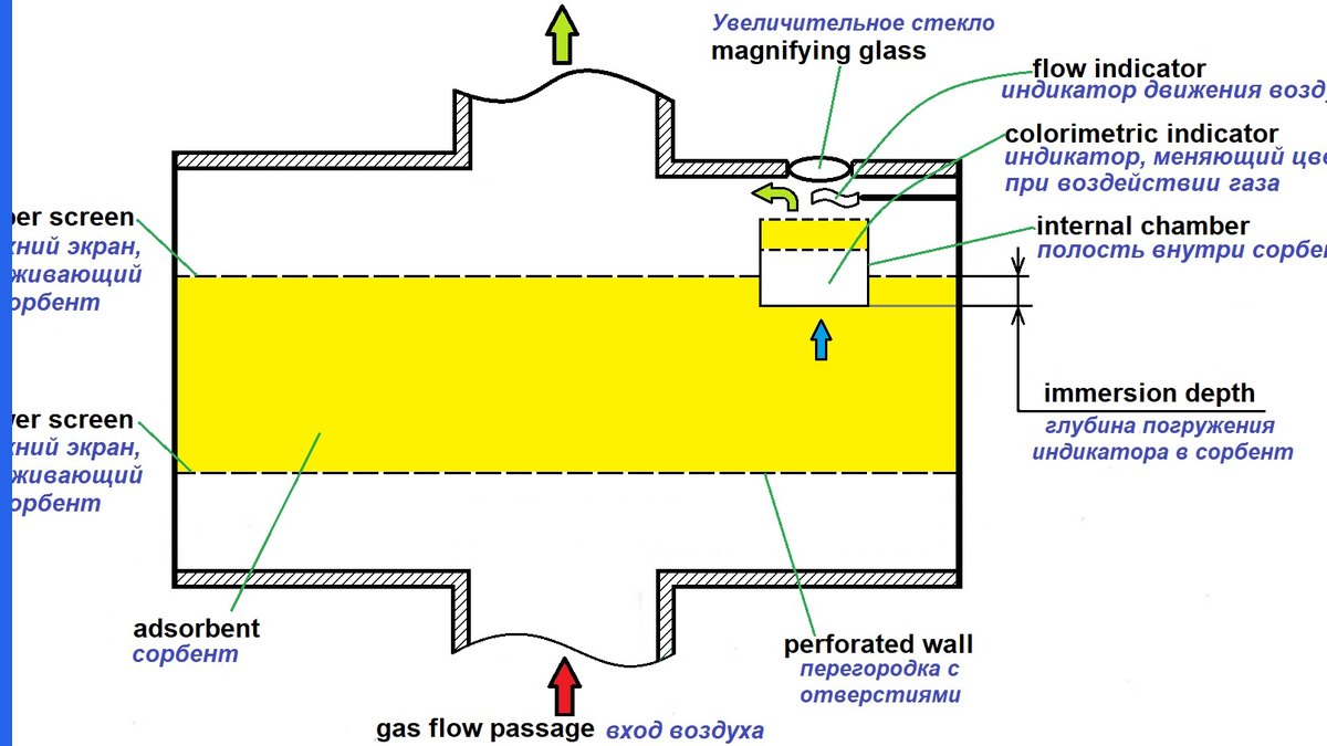
Most drawing objections in chip cases are not about accuracy. They are about legibility after reduction. A device cross-section carries ten or fifteen stacked regions, each of which needs to be visually distinct, individually labelled, and still readable when the Office shrinks the sheet. Mechanical drawings rarely stack anything; chip drawings stack everything.
The second structural difference is proportion. A gate oxide a few nanometres thick sits beneath a metal stack hundreds of nanometres tall. Drawn to scale, the dielectric disappears. Drawn legibly, the figure is wildly out of proportion. That tension sits behind most of what follows.
The third is the evidence problem. For a novel crystalline phase or an interface morphology, a line drawing may genuinely not be the best disclosure available. The rules allow for that, but only on specific terms.
Rule 1: Hatch every section, and hatch materials differently
Cross-sections are the workhorse figure in chip practice, and 37 CFR 1.84(h)(3) is explicit about how they are rendered. Hatching must be used to indicate section portions of an object, and it must be made by regularly spaced oblique parallel lines spaced sufficiently apart to enable the lines to be distinguished without difficulty.
Two phrases there do the work. Regularly spaced oblique parallel lines rules out the solid fills and grey tones that CAD and layout tools produce by default. Distinguished without difficulty is a legibility test, and it is the one chip figures fail, because a draftsperson trying to differentiate twelve layers reaches for ever-finer hatching until adjacent regions merge into grey.
The practical discipline is to assign hatching by material class rather than by layer index, and to cap the number of distinct patterns in any one figure. Where a stack genuinely needs more distinctions than hatching can carry, split it across a detail view instead of compressing it into one sheet.
- Oblique parallel lines only — not stipple, not solid black, not a grey wash
- Consistent hatching for the same material across every figure in the application
- Spacing wide enough to survive reduction, which in practice means wider than looks right on screen
- A detail view rather than finer hatching when a stack runs out of distinguishable patterns
Rule 2: Draw for the two-thirds reduction, not for the screen
37 CFR 1.84(k) sets the scale requirement, and it is a legibility floor rather than a fidelity requirement: the scale to which a drawing is made must be large enough to show the mechanism without crowding when the drawing is reduced in size to two-thirds in reproduction.
This is the rule that licenses the out-of-proportion layer stack. The regulation does not ask whether the figure is dimensionally faithful to the device. It asks whether the mechanism is still readable after a one-third reduction. A monolayer drawn thick enough to see is compliant; a monolayer drawn to scale and therefore invisible is not, because the claimed feature has effectively vanished from the figure.
Test it the way the Office will see it. Print the sheet, reduce it to two-thirds, and look at the places where hatching meets hatching and where lead lines meet a layer boundary. If anything merges, the fix is wider spacing or an enlarged detail view, not a thinner line.
The companion requirement is in 37 CFR 1.84(l): every line, number and letter must be durable, clean, black, sufficiently dense and dark, and uniformly thick and well-defined. Anti-aliased exports from layout tools routinely violate that sentence — the edges come out grey and variable in width. Our note on patent drawing line thickness covers how to get a clean black line out of a CAD pipeline.
Rule 3: Reference characters need room the hatching will not give them
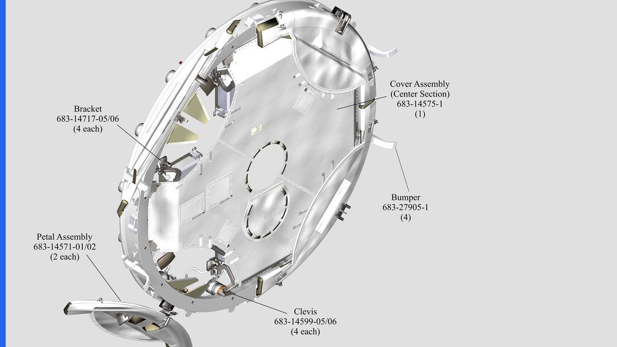
Under 37 CFR 1.84(p)(3), numbers, letters and reference characters must measure at least 0.32 cm (1/8 inch) in height. That is a fixed floor, and it does not bend because the figure is crowded.
In a fifteen-layer stack, a 1/8 inch numeral simply will not fit inside a thin region. The answer is lead lines out to a clear margin, not smaller type. Place the characters outside the hatched area, keep the lead lines short and non-crossing, and leave a small break in the hatching where a lead line terminates so the arrowhead is unambiguous.
Consistency across figures matters more here than in most fields, because a chip application often shows the same stack at six process stages. If region 104 is the barrier liner in Figure 2, it must be the barrier liner in Figures 3 through 7. Our guide to patent drawing reference numerals sets out the numbering conventions that keep a long figure set coherent.
Rule 4: Micrographs are allowed, but only as the only practicable medium
This is where chip practice diverges most sharply from the default advice. 37 CFR 1.84(b)(1) starts from a prohibition: photographs, including photocopies of photographs, are not ordinarily permitted in utility and design patent applications. It then supplies the exception that matters — the Office will accept photographs if they are the only practicable medium for illustrating the claimed invention.
The regulation lists examples of acceptable subject matter, and two of them are directly relevant to semiconductor work: photomicrographs and crystalline structures are both named. An SEM or TEM image of an interface morphology, a grain structure, or a novel crystalline phase therefore has a route in, provided the application explains why a line drawing could not carry the same disclosure.
Do not treat that as a general licence. A micrograph of a structure you could perfectly well draw invites an objection, and it buys nothing: a drawing is clearer and easier to amend. Use micrographs where the point being disclosed is morphological and genuinely resists line art, and include a drawn cross-section alongside wherever you can.
Colour is a further step. Under 37 CFR 1.84(b)(2), colour photographs must satisfy the conditions for both colour drawings and black-and-white photographs. The colour drawing route in 37 CFR 1.84(a)(2) requires a petition, the fee set by 37 CFR 1.17(h), the required drawing sets, and an amendment adding the prescribed language to the specification. A false-colour EDX map is a colour photograph for these purposes, so budget the petition — or supply a greyscale version that stands on its own.
Rule 5: Process claims need flow figures, and the rules cover them
A fabrication method claim is a sequence, and a sequence is best shown as a flow figure or as a series of stage cross-sections. Both are legitimate, and chip applications usually need both: the flowchart for the claimed order of operations, the staged sections for what the wafer looks like after each one.
37 CFR 1.84(d) is the provision that admits the non-pictorial figures chip cases rely on. Chemical or mathematical formulae, tables and waveforms may be submitted as drawings, and are subject to the same requirements as drawings. That sentence brings an I–V curve, a C–V sweep, a doping profile and a process parameter table inside the drawing rules — which means the 1/8 inch character height, the black uniform lines and the two-thirds legibility test all apply to them too.
The frequent oversight is axis labelling. A doping profile with 6-point axis text is a drawing violation, not a formatting preference. Our piece on patent diagrams for flowcharts and waveforms works through how 1.84(d) applies to graph and flow figures in detail.
Keep the content test in view alongside the form rules. 37 CFR 1.83(a) requires the drawings to show every feature specified in the claims. In a process case that means each claimed deposition, etch or anneal step needs to be locatable in the figures, which is exactly what a staged cross-section set delivers.
Rule 6: Shading helps, until it costs you legibility
37 CFR 1.84(m) is permissive and conditional at the same time: the use of shading in views is encouraged if it aids in understanding the invention and if it does not reduce legibility. Both halves are operative.
In chip figures, shading earns its place on three-dimensional views — a FinFET perspective, a through-silicon via, a stacked package — where it communicates contour that a flat section cannot. It costs you on cross-sections, where it competes directly with the hatching that 1.84(h)(3) already requires. Shading a hatched region twice over is the fastest way to produce a grey block.
The practical rule is to shade perspective views and hatch sections, and not to do both in the same region of the same figure. Our detailed treatment of patent drawing shading requirements sets out which shading techniques hold up under reduction, and the companion piece on patent drawing sectional views covers section lines and view alignment.
Rule 7: The form rules change the moment you leave the USPTO
Chip portfolios are filed internationally almost by default, and the drawing rules abroad are not the CFR.
For an international application, the governing provision is PCT Rule 11, applied by the receiving Office and the International Bureau. It is broadly similar in spirit to 37 CFR 1.84 but differs in detail on margins, sheet numbering and the text permitted in figures, and a drawing set that passes a US formalities review can still draw a PCT defect notice.
Europe is the trap, because the rule most sources still cite no longer exists. Rule 46 EPC, which set the form of the drawings, was deleted with effect from 1 February 2023, following the Administrative Council decision taken at its 172nd session on 13 October 2022. Paragraphs (3) to (12) of Rule 49 EPC went with it. The presentation requirements were moved into a Decision of the President of the EPO so that they can be updated as the Office’s digital systems change, with Rule 49 retained as the enabling provision. The working text for drafters is now the President’s Decision together with the EPO Guidelines for Examination, Part A, Chapter IX.
If your drawing standards document still says “Rule 46 EPC”, it has been out of date for over three years. Our summary of the current EPO Guidelines A-IX drawing rules reflects the post-2023 position, and the PCT drawing requirements guide covers Rule 11 in full.
One more route is worth flagging. Package and chip-module appearance can be protected by design patent, where the drawings are the claim. 37 CFR 1.152 requires the design to be represented by a drawing complying with 1.84, with appropriate and adequate surface shading to show the character or contour of the surfaces, and broken lines used to show visible environmental structure but never hidden planes and surfaces.
A pre-filing check for a chip figure set
Run this before the application leaves your desk. It catches the objections that semiconductor patent drawings attract most often.
- Print at full size, reduce to two-thirds, and confirm nothing merges — the 37 CFR 1.84(k) test
- Confirm every section is hatched with oblique parallel lines, and that the same material carries the same hatching in every figure
- Measure the smallest reference character; it must be at least 0.32 cm (1/8 inch)
- Walk the claims and point to each recited feature in a figure, as 37 CFR 1.83(a) requires
- Check that no layer thin enough to be claimed has been drawn to scale into invisibility
- Justify every micrograph as the only practicable medium, and price the petition and 1.17(h) fee for any colour figure
- Confirm axis text, table text and legends on 1.84(d) graphic forms meet the same character height as the drawings
- Re-check the European set against the President’s Decision and Guidelines A-IX, not the deleted Rule 46 EPC
Semiconductor portfolios are also where drawing quality shows up commercially. Figures get read closely in diligence and in licensing negotiations — our notes on semiconductor cross-licensing and patent risks in semiconductor M&A show how often a figure set is the first thing a counterparty examines.
Have Your Chip Figures Checked Before You File
PerspireIP prepares and corrects cross-sections, staged process figures, flow diagrams and design-patent views for semiconductor applications, to USPTO, PCT and current EPO presentation standards. Send us a GDSII export, a layout screenshot, a TEM image or the formalities notice you need answered. See our patent drawing services or contact us for a scope and turnaround estimate.
Frequently Asked Questions
Can I file SEM or TEM images instead of drawings in a semiconductor patent application?
Only where they are the only practicable medium for illustrating the claimed invention, which is the standard set by 37 CFR 1.84(b)(1). The regulation specifically names photomicrographs and crystalline structures among acceptable subjects, so interface morphology and novel crystalline phases have a genuine route in. Explain the necessity in the application, and supply a drawn cross-section alongside wherever one is possible.
Do semiconductor patent drawings have to be to scale?
No. 37 CFR 1.84(k) requires the scale to be large enough to show the mechanism without crowding when the drawing is reduced to two-thirds, which is a legibility standard rather than a dimensional one. Drawing a nanometre-scale dielectric thick enough to see is therefore correct practice, while drawing it to scale and rendering it invisible risks losing a claimed feature from the figures.
How many different hatching patterns can one cross-section carry?
There is no numerical limit, but 37 CFR 1.84(h)(3) requires oblique parallel lines spaced sufficiently apart to be distinguished without difficulty, and that is what caps it in practice. Once adjacent regions stop reading as distinct after a two-thirds reduction, the figure fails. Split the stack into a detail view rather than reaching for finer hatching.
Is Rule 46 EPC still the European drawing rule?
No. Rule 46 EPC was deleted with effect from 1 February 2023, along with Rule 49(3) to (12), following the Administrative Council decision of 13 October 2022. The presentation requirements now sit in a Decision of the President of the EPO, with Rule 49 as the enabling provision, and the working guidance is the EPO Guidelines for Examination, Part A, Chapter IX.
Do I need a petition for colour figures in a chip application?
For a colour drawing, yes — 37 CFR 1.84(a)(2) requires a petition, the fee under 37 CFR 1.17(h), the required drawing sets and an amendment adding the prescribed language to the specification. A colour photograph such as a false-colour EDX map must satisfy the conditions for both colour drawings and black-and-white photographs under 1.84(b)(2). Supplying a greyscale figure that stands on its own avoids the whole process.
Do process flowcharts and I-V curves count as patent drawings?
Yes. 37 CFR 1.84(d) provides that chemical or mathematical formulae, tables and waveforms may be submitted as drawings and are subject to the same requirements as drawings. That brings doping profiles, I-V and C-V plots and parameter tables within the character-height, line-quality and legibility rules, which is why axis text set in small type is a drawing defect rather than a styling choice.